The NEST group has recently secured considerable research funding and hosts state of art research facilities; these include electron beam lithography, nanoimprint lithography, optical lithography, laser mask writer, atomic force microscopy, reactive ion etching, and various physical deposition equipments. The group is part of the MacDiarmid Institute for Advanced Materials and Nanotechnology, a National Centre of Research Excellence. A number of scholarships are regularly available, please contact relevant staff.
What is Nanostructure Engineering Science and Technology?
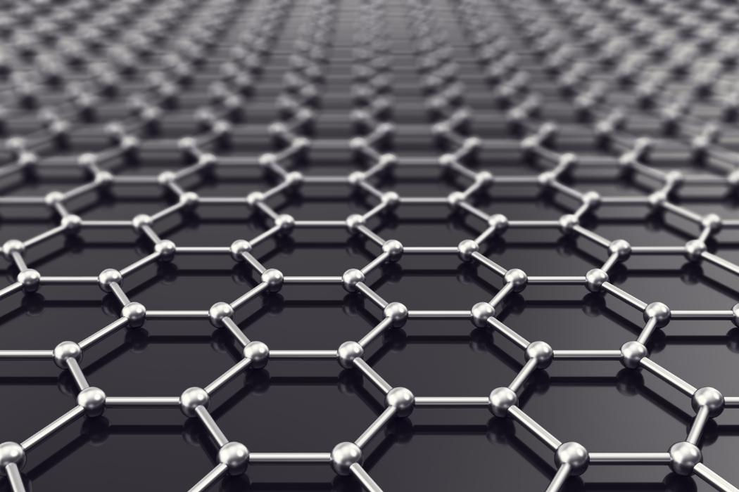
The forefront of much modern engineering and science research is at the scale of the smallest devices currently possible - in the range of nanometres. For engineers, the advantages of such small devices include increased speed and packing density, and novel functionality. For the scientist, working on such small scales reveals a range of exciting and unexpected fundamental phenomena.
Ideally engineering and scientific developments feed off each other: The NEST group performs advanced research in niche areas across the spectrum of applied engineering and basic science of nano-metre scale structures. The group focuses on fabrication and characterisation of nano-scale electronic, opto-electronic and micro/nanofluidic devices.
The Nanostructure Engineering, Science and Technology group (NEST) based at the University of Canterbury invites applications from well qualified graduates in Physics, Electrical Engineering, or a related subject, to carry out research towards a masters degree or PhD in nanotechnology.
The NEST group regularly delivers on research related to projects funded by the Marsden fund, Ministry of Business, Innovation & Employment grants and Centres of Research Excellence. The programme involves collaborations with University of Otago, Victoria University of Wellington, University of Auckland and Callaghan Innovation; some projects are based at those institutions or will involve collaborative work with them. A number of studentships are available, covering tuition fees at the domestic rate and living expenses at a reasonable level.
See the Research Projects page for more information about the current research
Micro- and Nanofabrication Facilities
Cleanroom Facility for micro- and nanofabrication are housed in the Electrical and Computer Engineering Department. The facility is equipped for thin-film deposition, thermal processing, photolithography (yellow room) including mask fabrication, nanoimprint lithography, electron beam lithography, wet etching, dry etching (reactive ion etching) and materials characterization.
Equipment
- Laurell WS-650 and Headway PWM32-PS-R790 spin-coaters
- EVG automated NIL system
- Heidelberg uPG101 laser mask writer
- LEO FEG-SEM & Raith150 electron beam lithography system
- Karl Suss MA-6 UV / DUV mask aligner
- Nanoscribe Photonic Professional GT2 nanoscale 3D printer
- Silicon tube furnaces
- Reactive ion etching Oxford Plasmalab 80
- Edwards Auto500 DC/RF magnetron sputtering system
- Temescal FC-1800 electron beam evaporator
- Oxford PlasmaPro 100 Cobra ICP deep reactive ion etcher
- Tergeo remote and immersion plasma cleaner
- Optical profilometer Profilm3D
- Stylus profilometer Taylor-Hobson Intra-Touch
- Atomic force microscope Digital Instruments Dimension 3100
- Optical microscope Olympus BX30
- Interference lithography
- Micromill CNC Mini-Mill/GX
- Semiconductor device characterisation HP 4155A parameter analyser
- Kulicke and Soffa ultrasonic wirebonder Model 4526
- Cascade Microtech 11000 probe station with Temptronic TP03000 thermal chuck
- ABET Sun3000 solar simulator
- FR-pOrtable non-destructive characterization of transparent and semi-transparent single films or stack of films
- Datron Neo 2 CNC mill
- Henniker HPT-200 benchtop plasma treatment system
Microfluidics and Cell-culture Facilities
PC-2 Biological Containment Facility certified for live cell and micro-organism experiments. Equipped for cell-culture, biological imaging and microfluidic device testing.
Equipment
- Class 2 Biological Laminar Flow Hood
- 2x Harvard PHD2000 Syringe Pump
- NE4000 Syringe Pump
- 2x Elveflow OB1 MK3+ - 4 channel flow controller
- Elveflow MUX Quake Valve - microfluidic flow switch matrix
- Elveflow flow and pressure sensors
- Nikon Eclipse 80i Fluorescence Microscope (B-3A, FITC, TxRed, DAPI, Special Red, RTDP, MitoXpress)
- Nikon Eclipse Ti Inverted Fluorescence Microscope
- Hamamatsu ORCA Flash 4 V2 digital imaging system
- LED microscope illumination X-Cite-120LEDBoost
- Nikon Eclipse TS100 F Inverted Microscope
- Contherm Mitre 4000 Cell-Culture Incubator
- Heraeus Labofuge 300
- PreSense Microx4 trace dissolved oxygen sensor system
- Autolab Potentiostat PGSTAT302 with FRA32M, ECD, FI20 and BA modules
- Electro-Technic Products BD20 Corona Plasma Treater
- Thorlabs High-Speed Motorized XY Scanning Stage
Academic Staff
- Martin Allen
- Volker Nock
- Paul Gaynor
- Ciaran Moore
- Maan Alkaisi
- Simon Brown
- Roger Reeves
- Debbie Munro
- Paula Brooksby
Post-Doctoral Fellows
Researcher Engineers
Postgraduate Students
- Daniel Mak
- Zhuoyue Wang
- Debolina Sarkar
- Ryan Adams
- Kate Wislang
- Sarah Sale
- Claudia Allan
- Finn McIntyre
- Rhys Marchant-Ludlow
- Jude Kalan
- Claudia Allan
- Marsden Fund - The Marsden Fund was established by the government to support excellence in research and researchers
- Callaghan Innovation - New Zealand's leading industrial science and technology company with an international focus and reach
- The MacDiarmid Institute for Advanced Materials and Nanotechnology
- The Dodd-Walls Centre
- The Biomolecular Interaction Centre
Other Sites
- Micro-fabrication Facility - Callaghan Innovation
- Auckland Microfab - University of Auckland
- Cleanroom Fabrication Facility - Victoria University
- Photonfactory - University of Auckland
- The Australian National Fabrication Facility
- National Institute of Advanced Industrial Science and Technology, Japan
- The University of Glasgow Nanoelectronics Research Centre
The micro- and nanofabrication cleanroom facility of the Nanostructure Engineering Science and Technology group is used for outreach activities and undergraduate teaching. In particular, the facility is used to deliver the laboratory part of the 3rd professional year electrical and computer engineering course ENEL491 - Nano Engineered Devices. As part of this laboratory component students use NEST facility equipment to fabricate single crystal silicon solar cells and characterize their efficiency.
Current students please contact Linda Chen for training and laboratory access.
For advice
