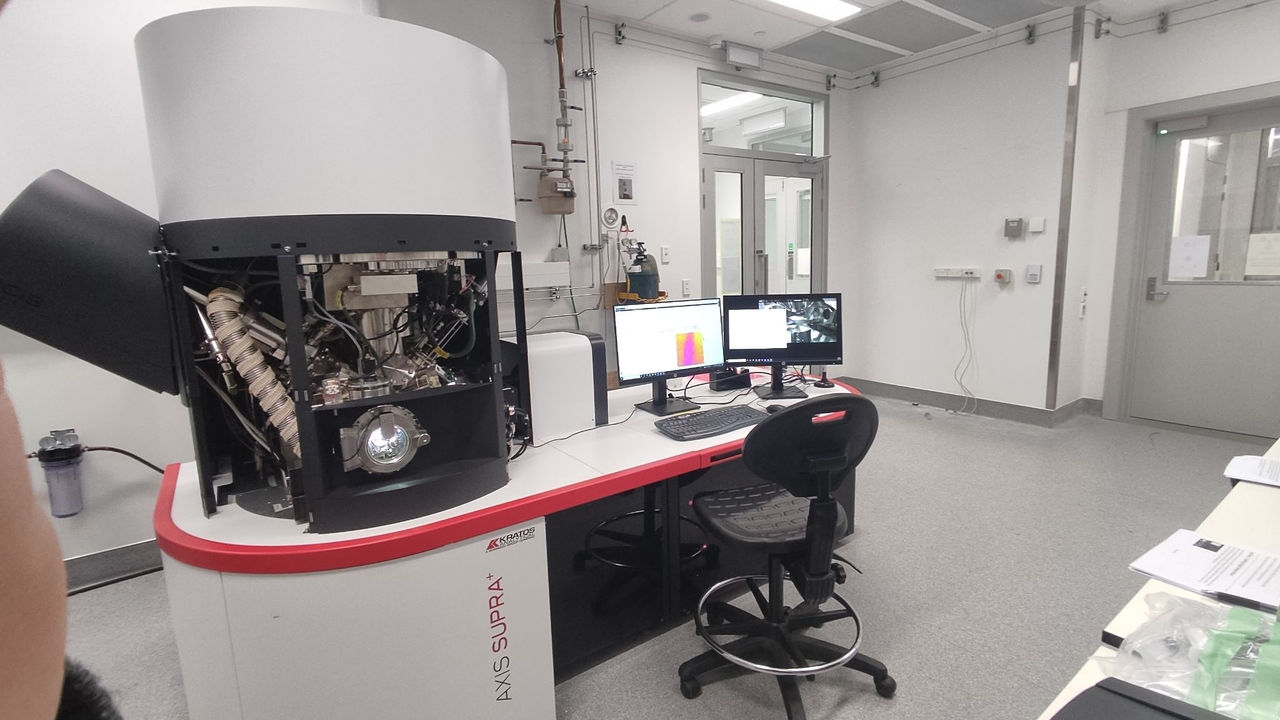


X-ray Photoelectron Spectroscopy (XPS) is a powerful surface analysis technique used to determine the elemental composition, chemical state, and electronic structure of materials. It works by irradiating a sample with X-rays, causing the emission of photoelectrons.
By measuring the kinetic energy of these electrons, we can identify the elements present, their bonding environments and obtain the material's unique signature.
XPS is widely used in materials science, nanotechnology, and semiconductor research, as it provides valuable insights into surface chemistry, oxidation states, and contamination levels. The technique is highly sensitive, analyzing only the top 1–12 nm of a material, making it ideal for studying thin films and coatings.
At our Advanced Materials facilities we can combine XPS with other processing and characterization techniques, to study samples from the nano-scale all the way up to macroscopic bulk materials in a single instrument.