

UC’s Nanofabrication Laboratory (NanoLab) is the most comprehensive of its kind in New Zealand. Hosted by the Department of Electrical and Computer Engineering, the facility provides access to micro- and nanofabrication technologies for a variety of academic and commercial users and supports undergraduate teaching in nanoengineering.
The facility is supported by the MacDiarmid Institute for Advanced Materials and the Biomolecular Interaction Centre, forming a major node as the national network of nanofabrication facilities. It consists of a central fabrication space with yellow room, a connected device-characterisation area and an adjacent physical containment level 2 (PC2) laboratory space for handling biological materials. Research conducted at the facility covers microelectronic devices and solar cells via sensors and actuators, micro-electromechanical systems, and microfluidic and lab-on-a-chip devices.
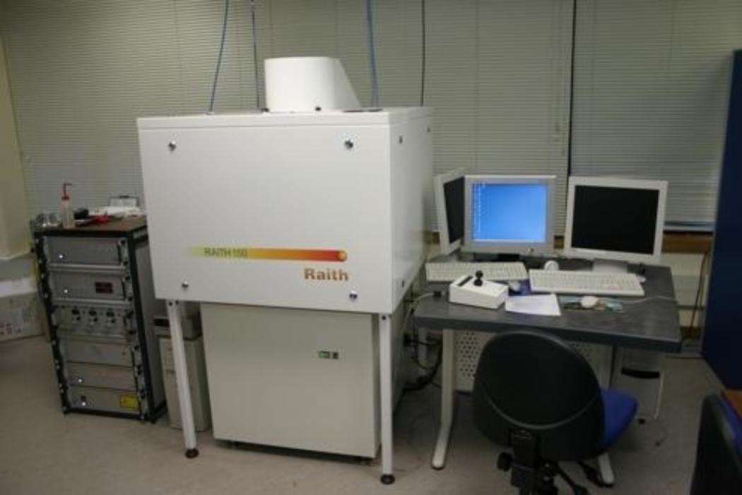
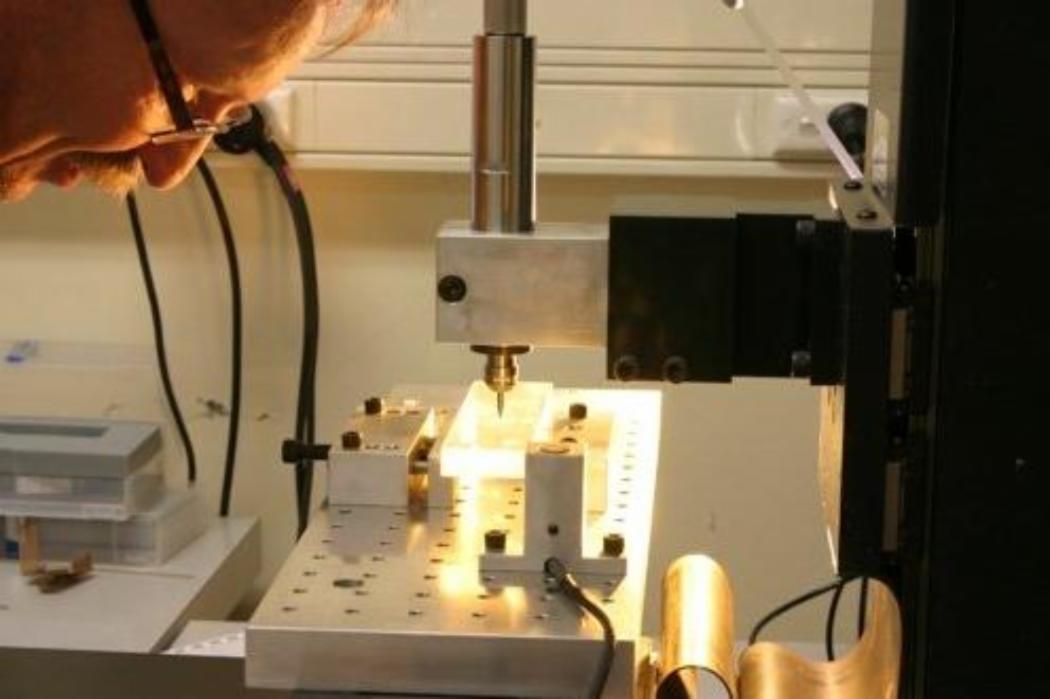
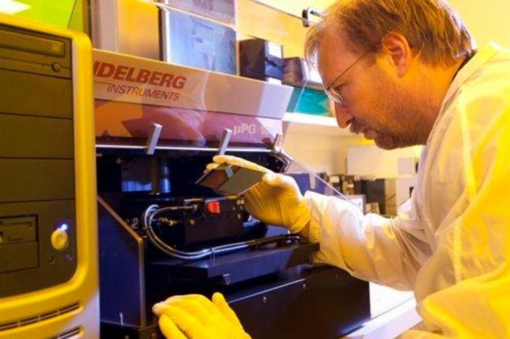
Available technologies range from semiconductor and advanced materials processing to the culture and maintenance of biological microorganisms on devices. Pattern-transfer techniques include laser mask writing, UV-based thin- and thick-film photolithography, laser interference lithography, electron beam lithography (Raith 150) and two-photon polymerisation 3D printing (Nanoscribe PPGT2) supported by spin-coating and wet-bench processing infrastructure.
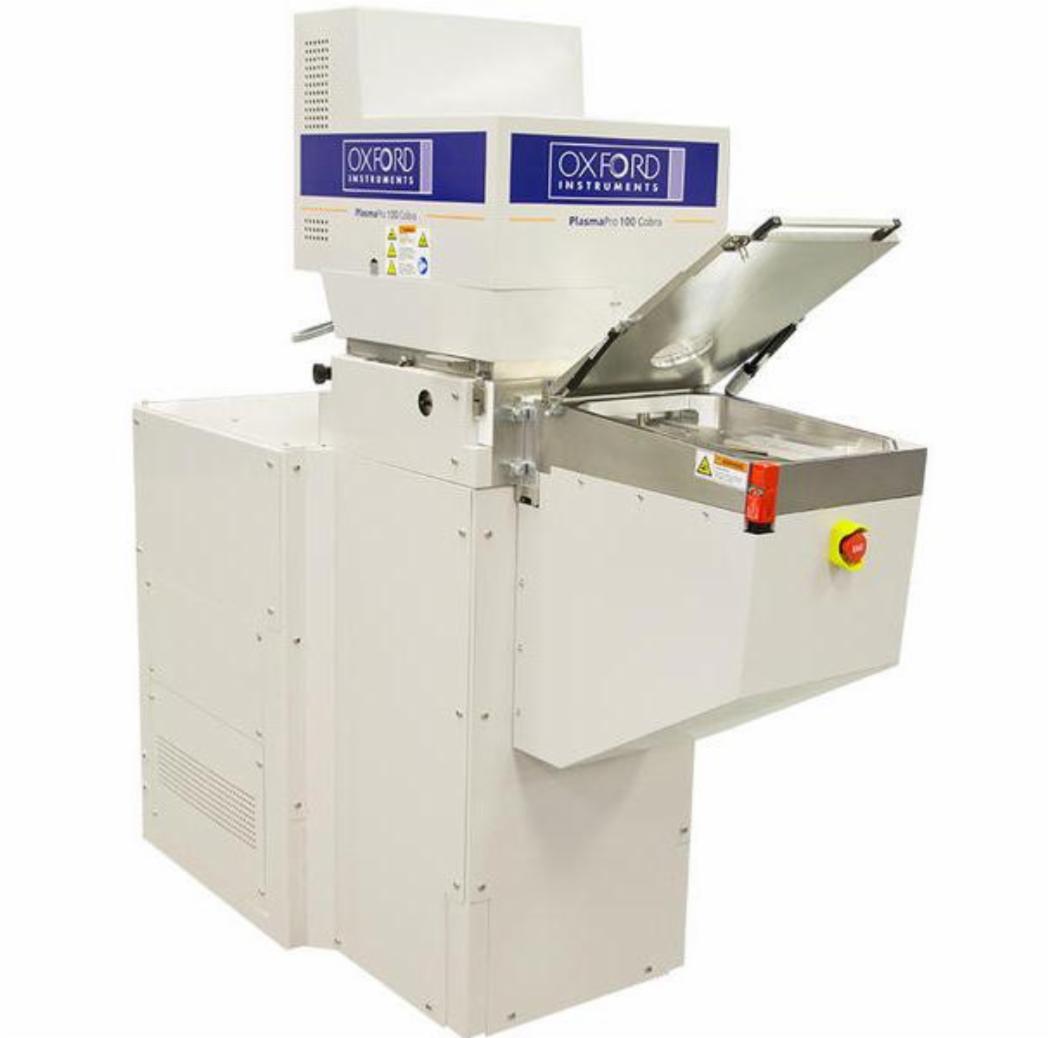
For film deposition, DC and RF plasma sputtering, electron beam and thermal evaporation, thermal growth and mist CVD are available. These are complemented for patterning by plasma etching, deep reactive ion etching (PlasmaPro 100 Cobra) and wet-etching.
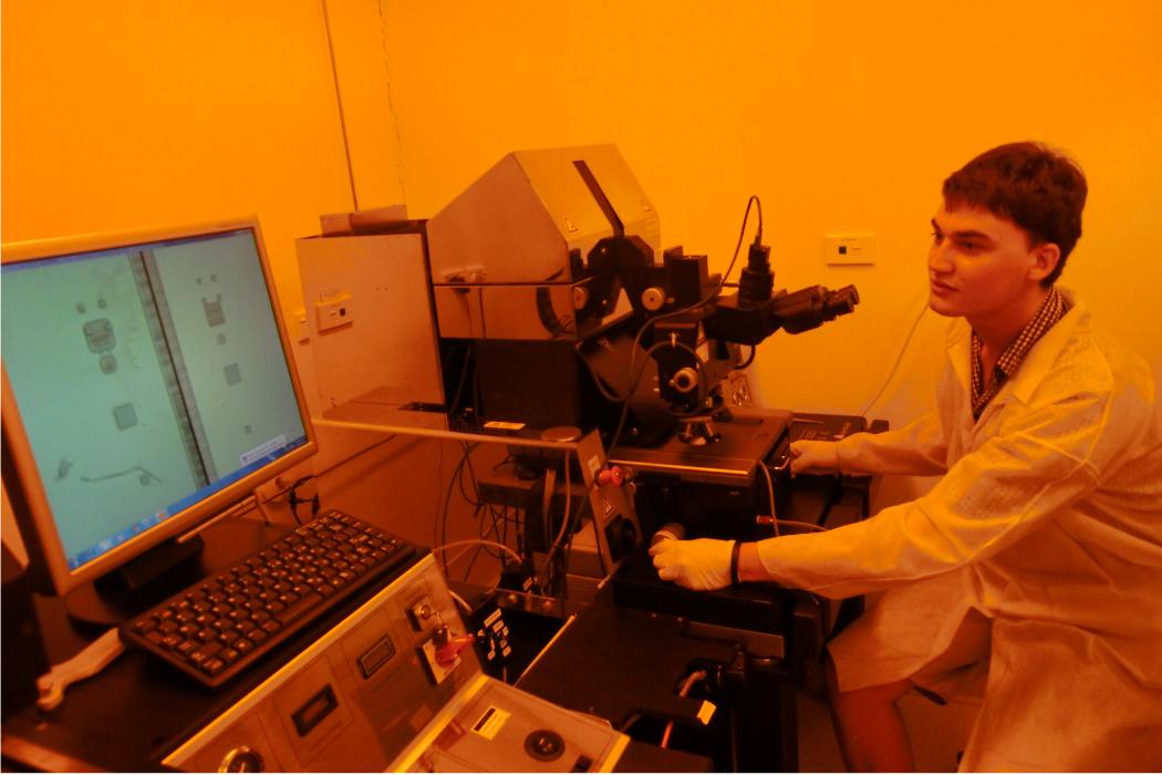
Back-end processing equipment includes wafer saws, a CNC micro-mill and wire-bonding. Material and device characterisation techniques include light-, scanning electron- and atomic force microscopy, optical profilometry, goniometry, ellipsometry, thermal spectroscopy (3w), a solar cell simulator, a Hall-effect setup and a probe station with semiconductor parameter analyser. In the biological applications space, mammalian cell-culture, live-cell and epi-fluorescence microscopy, microfluidic flow control and electroanalytical experimentation equipment are provided.
The facility is available to both research and commercial users. If would like to know more, please contact Associate Professor Volker Nock.